Multisim Tutorials
Hierarchy Block and Sub-Circuit Basics
Hierarchy Block and Subcircuit Basics
By Lacy
Hierarchy Blocks and Subcircuits are basically the same thing with the big difference being how they are handled by Multisim. A subcircuit block is contained totally within the current design project while a hierarchy block is saved as a separate schematic on your drive.
You create a subcircuit by three methods.
1. Creating a window around the components and nets in your schematic to be included in the subcircuit and then going to PLACE>Replace By Subcircuit. This creates all the input and output connections automatically. You may have to rename them later to something more desirable as they are just generically labeled as IO1, IO2 etc. Caution: This removes the components from the main schematic and places them inside the subcircuit. You can always use the Undo command to revert it back in case you made an error. I would suggest to do this immediately after creating it otherwise you run the risk of not being able to restore the original portion of the schematic without doing a lot of cutting,pasting and rewiring. This is due to the Multlsim Undo buffer having a limited size.
2. Going to PLACE>New Subcircuit. This creates a blank box without any input or output pins. You must click the subcircuit box and select Edit HB/SC and then place your circuit inside with HB/SC connectors from PLACE>Connectors>HB/SC Connector.
3. Create the schematic of your subcircuit first, place the HB/SC connectors and then use the process outlined in step one. To create a Hierarchy Block you can use the same 3 techniques oulined above except you choose from the Place Menu -Replace by Hierarchy Block-, -New Hierarchy Block-. The difference is that this block will be saved as a separate file on the hard drive and can be re-used in other designs or editied at anytime by loading it as a separate Multisim scheamtic. Subcircuits are saved within the current project and cannot be re-used in other designs.
So what are they good for? The subcircuits can have many uses, but the one that I use them for most often is to shrink my print down to create a block diagram form. This compresses the design to fit in my work space. Also, you could start out using subcircuit blocks to outline the block diagram for design flow purposes and then go into each subcircuit and create the circuit that accomplishes this particular block. There may be other applications for these, but this is mainly what I have used them for.
The Hierarchy blocks are more versatile in their applications. Once you create a circuit that may be used across more designs, then this will always be available to you to use from the hard drive. You could have a complete library of common circuits and then just choose the one you need and place it in the current design. This makes it easier to design things as you do not have to re-create circuits that have already been designed and tested. Call it Plug and Play Multism style.
You can also create components using the Hierarchy Blocks. This is not like using the Component Wizard, but is an alternative when you need a quick and dirty component for your design. This is the only method of component creating that allows the use of Interactive Components to be used in the creation of new parts.
Now for the downside of Hierarchy Blocks/Subcircuits. You cannot assign footprints to them for export to Ultiboard as a single component. All the components inside the subcircuit/hierarchy block will transfer as individual parts. If you need to export your subcircuit/hierarchy block as a single component to Ultiboard you will need to use the Component Wizard to create a blank component template with a footprint. Once the simulation phase is done you will need to replace the subcircuits in your schematic with the blank component templates in order to transfer your schematic to Ultiboard in this manner.
What I have outlined here is just the basics for these items. There may be more uses for them other than what I have outlined here. I only want to give the basics and you may have a completely different use for them. It is up to the designer and the application to determine how to use them and when.
How to Create a Multisim Component Model Using the Schematic Capture
1. Find the datasheet for your component.
2. If the datasheet has a internal schematic for the part then enter this information into the schematic capture portion of Multisim.
3. Simulate the schematic you have just drawn to ensure that the part is working according to what you expect it to using the normal procedure for simulating circuits.
4. Once you are satisfied that everything is working according to what you want. Then remove all voltage sources, input sources and instruments used to simulate the circuit.
5. Goto PLACE>Connectors>HB/SC Connector and select. Place these connectors on the input, output and Power, and Ground nets. Label them as per the datasheet.
6. Once this is complete then be sure to save your work in case your need to edit something later.
7. Now goto TRANSFER>EXPORT NETLIST and click it. A dialog box will come up. Enter the filename that wish to save with. This will create a file called "yourfilemame.CIR"
8. Now you are ready to create your component. Go through the normal procedure of creating a component. Once you get to the point where it asks for a model for this component select "load from file" and browse to the .CIR file you just saved and load it.
9. Now comes the tricky part and this must be followed exactly or it will not work. Go into the model file window and at the very beginning add the line
".SUBCKT (modelname) (pin1) (pin2) ..."
The pin names are what you called the HB/SC connectors in the original schematic. Then at the very end of the model file windowplace the statement .ENDS.
10. Make sure the Pin Mapping table is correct and after that you should have a functioning component.
This works good for components with schematics in the datasheet that are clear and concise. Some datasheets only give the internal schematic in block diagram form and this is not well suited for this technique as you really have no idea on what is inside the block in most cases.
Also, most datasheets do not list the type of transistors, diodes or anything like that so you will just have to approximate the type to use based on the datasheet specifications.
Also, please note that there can be no interactive components in your original schematic. Multism does not allow these components to be used to create other components. These include LEDs, Switches, Relays, MCU components.
Completing the Design with NI Multisim and NI Ultiboard: Annotation Fundamentals
The design once transferred to layout exists in two different (though integrated) applications. It is important that as a design engineer, the project be managed such that both in schematic and layout form, the topology be consistent.
This can be difficult to manage as changes can now occur both in Multisim and Ultiboard.
In order to facilitate the management of such changes, the integration between Multisim and Ultiboard allows you to annotate changes from one form of the design to the other.
Definition: Annotation is the transfer of design changes from schematic to layout, or layout to schematic.
In this article the transfer and annotation of changes in NI Multisim and NI Ultiboard is documented. This article provides a how-to-guide, tips-and-tricks as well as best practices on how to use the annotation process in the National Instruments Circuit Design Suite.
1. Introduction
Forward annotation is the process by which a designer transfers changes from a schematic to a PCB layout environment. Back annotation is the opposite of this procedure, when changes are made at the layout level and transferred back to the schematic.
Forwards and backwards annotation are import aspects of the design process. Changes that are made at every incarnation of a design should be appropriately merged into other design stages, so that iterative work is properly documented. This is important for both the present design process as well as future maintenance.
Many products are on the market for multiple years and elements of the design (such as components and devices) may become obsolete or require alteration during this time period. The need for incremental changes to a design means that a complete set of files which depict the design at both schematic and layout stages can avoid frustration and save time in the future.
Due to the importance of this task a designer should take great care to ensure that the schematic and layout of a design are completely in sync.
To forward and backward annotate changes in either the schematic or the PCB layout is a very simple and straight forward procedure, however to reduce the possibility of error it is important to understand how annotation works from the fundamental elements (the netlist) to the actual annotation procedure.
Accompanying this tutorial is a 7321_annotation.zip file which contains various examples to help in the tutorials in this article.
2. What is Annotation?
The forward and backwards annotation process is based upon the transfer of a netlist file. The netlist file is a text based representation of your design and as changes are made either at the schematic or layout level, it is through the netlist that this information is transferred. In this article we will investigate:
- How does a netlist facilitate annotation
- Transferring a file to layout
- Forward Annotation
- Backwards Annotation
3. What is a Netlist?
When a design is created in NI Multisim and NI Ultiboard, the components, devices, and net connections are automatically defined in an ASCII file. This ASCII file contains:
- The Reference IDs (which are unique identifiers) of design components
- Net names and connections between each device/component
When a user transfers this netlist from Multisim to Ultiboard a new netlist file with a .ewnet extension is created which contains:
- The name of the Landpattern (or footprint) associated with each Reference ID
- The unique pin names of each device
This netlist is the fundamental representation of a design, as well as the method through which the design can be transferred either from schematic to layout, or vice-versa.
4. Transferring from Multisim to Ultiboard
Before one can begin the iterative procedure of forward and backward annotation of design changes, the file must be transferred from the NI Multisim schematic capture environment to NI Ultiboard layout.
How to transfer a schematic to layout
With the following six steps we will transfer an example Multisim schematic to Ultiboard
- Open the Forward Annotate 1.ms10 example file
- In Multisim select Transfer > Transfer to Ultiboard 10
- Multisim instructs you to save a netlist representation of the file in a .ewnet format.
- Save the file to the default location in the same folder in which the original schematic was saved.
- Ultiboard automatically launches
- The Default Track and Clearances dialog box appears. Accept the default setting by clicking on the OK button.
- The Import Netlist Action selection dialog box appears. Accept the default setting (to import all components and nets) by clicking on the OK button.
The schematic has been transferred from Multisim to Ultiboard.
What exactly happens when a netlist is imported into Ultiboard?
When the netlist is imported from NI Multisim (as in the steps above), Ultiboard iteratively undergoes a four step procedure to:
- Locate the landpattern or footprint name of a particular device as it is defined in the netlist file
- Search the Ultiboard component database in order to locate the landpattern.
- Place the landpattern on the work area.
- Assign each pin on the placed landpattern to a net.
The above four step procedure is repeated by Ultiboard until all landpatterns are placed onto the work area and nets have been assigned to all pins.
5. Important Considerations
Throughout the design process, particularly through the transfer process, there are a number of events that can occur which can potentially cause errors. In order to help effectively handle these situations, the following section will outline a possible issue encountered in the transfer process. You will learn the correct procedure to resolve this issue.
Component not found during transfer … Part 1
When Ultiboard opens a netlist file it ascertains the name of a landpattern for a particular device and searches its database for a part that corresponds to this name to place on the work space. If a landpattern has been incorrectly named in the netlist or if it has not yet been created in the Ultiboard database then you have a situation in which a landpattern for a device cannot be correctly placed into the project.
To demonstrate what occurs when a landpattern cannot be found:
- Open Forward Annotate 1.ms10 in NI Multisim.
- Select Transfer>>Transfer to Ultiboard 10
- Multisim instructs you to save a netlist representation of the file in a .ewnet format. Save this file to the default location in the same folder in which the original schematic was saved.
- Ultiboard automatically launches
- The Default Track and Clearances dialog box appears. Accept the default setting by clicking on the OK button.
- The Import Netlist Action selection dialog box appears. Accept the default setting (to import all components and nets) by clicking on the OK button.
- Ultiboard is not able to locate one or more landpatterns defined in the netlist file within its database and therefore prompts the user with the following message:
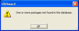
- Select the OK button to continue.
- Save the layout file as Forward Annotate 1.ewprj
When Ultiboard cannot find a component (as in this situation) it will map the element to a default square shape with multiple pins in order to not drop (or lose) nets and components due to an improper transfer. The default landpattern is shown below:
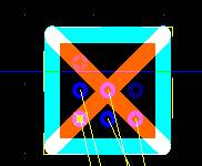
The red X through the landpattern indicates that the transferred landpattern name does not exist. In order to fix this situation and ensure that the change is properly reflected both at the schematic and layout level requires back and forward annotation.
We will now investigate what exactly back and forward annotation are, and will return to our above documented design error later in the article.
This error resolution is to be continued…
6. Forward Annotation
The Forward Annotation process is similar to a transfer to Ultiboard, however it transfers to a layout that already exists. This means that prior to forward annotation, a schematic has already been transferred to Ultiboard.
Forward Annotation only transfers incremental changes to the design to layout. Therefore it is not the entire design that is transferred, but only the changes in the schematic that have not yet been defined at the layout stage.
- Open Forward Annotate 3.m10 in NI Multisim
- Open Forward Annotate 3.ewprj with NI Ultiboard.
Previously the schematic was completed and transferred to layout. At this time we need to make additional changes to the schematic but must ensure that this change is properly represented at the layout level.
- Return to Forward Annotate 3.m10 in the Multisim environment
- Select LED1 and right click upon the device. Select copy from the short-cut menu.
- Paste the copied LED (named LED2) to the left of LED1 without connecting it to the design.
- Select R1 and right click upon the device. Select copy from the short-cut menu.
- Paste the copied resistor (named R5) to the left of R1 without connecting it to the design.
- Connect R5 and LED2 to the design according to the figure below.
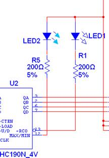
You have now changed your original design and must annotate these changes to layout. The following is the forward annotation process.
TIP: In order to safeguard your work it is always recommended to backup your layout file prior to a forward annotation. Before continuing make a backup of the Forward Annotate 3.ewprj file, saving it as Forward_Annotate_3_backup.ewprj
- Select Transfer>>Forward Annotate to Ultiboard 10 in Multisim
- Save the netlist to the default path.
- Click OK on the following warning message.

- Click OK on the Default Track and Clearances dialog box.
- Click OK on the Import Netlist Action Selection dialog
LED 2 and R5 are now merged into the Ultiboard layout and are placed outside of the board outline. These components can now be placed and configured as needed for the design.
7. Back Annotation
The Back Annotation process, like forward annotation, requires a schematic to have already been transferred to layout. After this primary step, back annotation allows an engineer to make changes at the layout stage and have these changes merge back into the schematic file.
Limitations
It is important to note that in making changes to your design, it is preferred (and advantageous) to forward annotate changes made in the schematic to Ultiboard. This is because the back annotation process does have limitations upon what changes can be effectively transferred back to the schematic.
What can you back annotate?
- A changed in the Reference ID of a component
- The new name for a net
- A deleted footprint
- A changed footprint
What can you not back annotate?
- Components added to the design
- A modified net connection between components
- A pin and/or gate swap
It is important to note these limitations, as a faulty back annotation can create schematics out-of-sync with layout. In larger designs where a back annotation may not be glaringly obvious, this can become an issue overlooked which can cause major issues in a design.
How to Back Annotate
To demonstrate how to back annotate we will begin making some changes to our design to annotate back to the schematic.
- Open Back Annotate 1.ewprj in Ultiboard.
- Open Back Annotate 1.ms10 in Multisim
Changing the name of all the landpatterns (or footprints) in the design:
- In Ultiboard select Tools>>Renumber Footprints.
- Apply the default renumbering settings by clicking on the Apply button. All landpatterns will now be renamed in a logical order based upon the settings of the dialog box.
Deleting a device:
- In the Ultiboard file locate the LED1 landpattern. Select the device and delete if from the layout.
Changing the landpattern dimensions of a device:
- Locate the C2 device.
- Select Tools>>Change Shape. In the NI Ultiboard database locate the CAPC0603X33N landpattern (this can be found in the Surface Mount Technology – Capacitors – SMD hierarchy).
- In the database dialog and click the OK button to replace the landpattern in the work area.
- There are three similar footprints in the work area you will be asked if you wish to replace them all, select Yes.
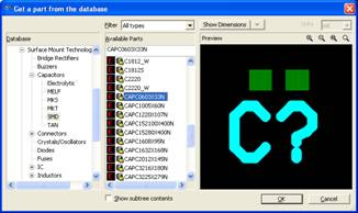
Having completed all of the changes to the layout file we are now ready to back annotate.
- Select File>Save in Ultiboard.
Ultiboard creates a log of all the changes made since last saving. These changes (documented in a log file) is saved in the same folder as the Ultiboard design file.
- Return to the Multisim environment in which Back Annotate 1.ms10 is already open.
- Select Transfer>>Back Annotate from Ultiboard to annotate the changes from Ultiboard.
- A dialog box will open in which to select the annotation log file. Navigate to the Back Annotate 1.log file and click on the Open button.
- A summary of all the changes made in Ultiboard appears. Click OK to approve the changes.
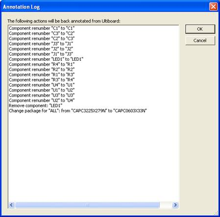
- A Notepad session will open to provide a summary of what was done to the Multisim schematic.

A component not found during transfer…part 2
In our first example in this article we had encountered a situation in which a landpattern that was to be transferred from Multisim to Ultiboard could not be found within the Ultiboard database, and therefore a default “landpattern missing” shape has been placed into the layout.

With a better understanding of how to forward and back annotate we can now fix this issue with these important design tools.
To fix this problem you have two options, replace the unknown landpattern/footprint in Ultiboard and back annotate the change or make the change in Multisim and forward annotate the new landpattern.
Back Annotation from Ultiboard
With the back annotation approach we must select a new footprint/landpattern from the NI Ultiboard database and merge this back into our original schematic.
- Return to Forward Annotate 1.ewprj.
- Click once upon the “unknown shape” to select it
- Select Tools>Change Shape.
- In the part selection dialog locate the SO8S landpattern from the Master database.
TIP: Under Available Parts field start typing SO8S and as you type Ultiboard filters out all footprints that do not contain the letters that was typed making component search much easier.
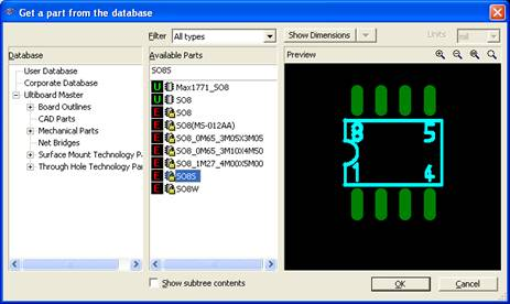
- Highlight the SO8S and press the OK button to replace the unknown shape.
It is now time to back annotate the change to the Multisim schematic.
- Select File>Save in Ultiboard.
- Ultiboard creates the log file of changes to the design.
- Return to the Multisim environment in which Forward Annotate 1.ms10 is already open.
- Select Transfer > Back Annotate from Ultiboard to annotate the changes from Ultiboard.
- A dialog box will open in which to select the annotation log file. Navigate to the Forward Annotate 1.log file and click on the Open button.
Forward Annotation from Multisim
We will now make the same change, but use the forward annotation process to have the same result.
- In Forward Annotate 1.ms10, locate the U4 component in the schematic.
- Double-click on U4.
- Select the Edit Footprint button.
- Click on the Select From Database button.
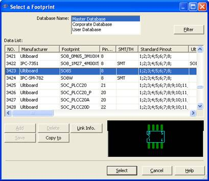
- In the Select a Footprint dialog, select the Master database.
- Scroll through the dialog box to locate the SO8S landpattern.
- Select SO8S and click on the Select button.
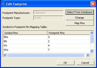
- DOUBLE CHECK the symbol to footprint mapping table to ensure that the symbol pins are correctly mapped to the footprint pins. If the mapping table is incorrect in here, your final product will not work.
- Click on the OK button.
- Select Transfer>>Forward Annotate to Ultiboard 10 in Multisim
- Save the netlist to the default path.
- Click OK on the following warning message.
- Click OK on the Default Track and Clearances dialog box.
- Click OK on the Import Netlist Action Selection dialog
The changes will now merge into the layout, and again you have successfully annotated changes.
8. Important Considerations
It is important to note that if in Ultiboard a change is made (for example a part deleted) and saved, that change is logged within the log file. If however at this point an undo is done upon the change (Edit > Undo …) and is again saved, the log file will not represent the undo. Therefore, if a back annotation procedure is done the component originally deleted in the first step will be annotated into the design.
The following exercise showcases the steps to recreate such an issue for clarification.
- Open Back Annotate 2.ewprj
- Locate and select the capacitor C3 on the design
- Press the Delete key on your keyboard
- Select File>Save. NI Ultiboard will create a Back Annotate 2.log file
- Select Edit>Undo and C3 should reappear on the design.
- Select Tools>Renumber Footprints and click OK
- Select File>Save and NI Ultiboard will update the log file previously created
- Startup NI Multisim and open Back Annotate 2.ms10
- Select Transfer>Back Annotate from Ultiboard
- Locate the log file and select it.
- Click on Open
- Review the summary report and notice that C3 was not back annotated.
When Undo was performed in step 5 above Ultiboard placed C3 back on the design but the log file was not updated. The Undo action in this case is similar to adding a new landpattern in the Ultiboard design. As mentioned earlier NI Multisim does not back annotate landpatterns added in the layout.
To avoid this situation, it is good practice to always modify changes such as landpatterns changes, schematic connections, pin names etc… in NI Multisim and then forward annotate to NI Ultiboard.
Creating a Custom Component in NI Multisim
Creating a Custom Component in NI Multisim and Creating a Custom Component in NI Ultiboard are your resources on how to intuitively and quickly learn how to create your own custom components.
Introduction
This tutorial is the first in a series of articles on component creation in NI Multisim and NI Ultiboard.
The purpose of this tutorial is to explain how you can create your own components for simulation and/or Printed Circuit Board (PCB) layout from within Multisim. You will create the component and then verify its operation. The Component Wizard is the primary tool used to create custom components in Multisim, and it walks you through all of the steps required to create a new component. Components details include symbol and optionally pin, model, and footprint information. Steps in the creation process include:
- Entering component information.
- Selecting a footprint and the component configuration.
- Selecting and/or editing the component symbol.
- Setting pin parameters.
- Mapping the symbol pins to the footprint pins.
- Selecting the simulation model.
- Mapping the symbol pins to the model pins.
- Saving the part in the database.
The tutorial steps you through the process of creating a simulation and PCB layout compatible component in Multisim. In the interest of completeness, you will learn how to create an advanced component with two sections. You will create a part with two schematic symbols, two models, but only one footprint. Many components are easier to create and not all steps outlined are required under most circumstances. Multisim also allows users to create simulation-only or layout-only components.
Part 2 of the component creation articles, entitled Creating a Custom Component in NI Ultiboard, outlines how to create a custom Ultiboard landpattern for layout. This landpattern is created manually so as to precisely define the shape, size, and dimensions of a Surface Mount Device (SMD). This footprint can be added to the Multisim database to define a custom component.
Single Section versus Multi-section Components
A single-section component is any component that has a single device per chip. A multi-section component is a component that has multiple gates or devices per chip. Examples of multi-section devices include logic gates or operational amplifiers. Letters, increasing from A-Z, enumerate the devices within multi-section components.
Simulation-only Components
Simulation-only components are designed to help verify designs; they are not transferred to board layout. There is no footprint information associated with them, and their symbols are colored black by default in the Multisim environment to easily identify them. An example of a simulation-only component is an ideal voltage source.
Layout-only Components
Layout-only components do not contribute to a simulation. They have no associated SPICE or behavior model. When connected parallel to the circuit, they will have no impact on the simulation. When connected in series, they will create an open circuit. Layout-only components are green on the Multisim environment. An example of a Layout-only component is a connector.
Creating a Texas Instruments® THS7001 Component in NI Multisim
The Texas Instruments® THS7001 is an example of a multi-section component. This component has a programmable gain amplifier (PGA) with a separate pre-amplification stage presented in a single integrated circuit (IC) package. In this package, both sections share power and reference voltage connections. The programmable gain is digitally controlled via three TTL-compatible inputs. For more details about this component refer to the file datasheet_ths7001.pdf located in the Downloads section.
In the next steps, you will learn to use the Component Wizard to create the THS7001 in Multisim.
Step 1: Enter Initial Component Information
- Select Tools»Component Wizard from the Multisim main menu. The Component Wizard window opens.
- Configure this window as shown in the following figure.
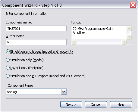
Figure 1. THS7001 component information.
- Click Next to continue.
Step 2: Enter Footprint and Package Information
In this step you will enter the footprint information. According to the datasheet, this component uses the HTSSOP-20 PowerPAD (PWP) footprint. You will select this footprint from the Multisim Master Database.
- Click on the Select a footprint button. The Select a Footprint window opens.
- Select the Master Database in the Database name listbox.
- Click Filter. This helps you do a quick search within the thousands of footprints.
- Click the Add row button.
- Configure the Filter window as shown in Figure 2.
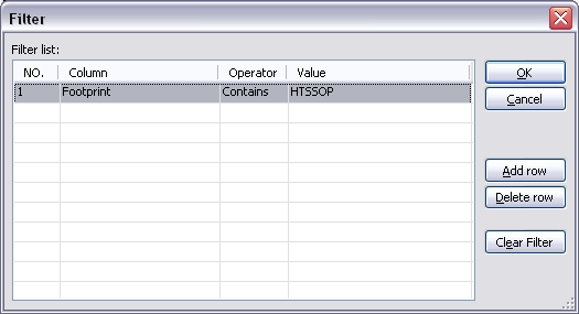
Figure 2. Filtering footprints.
- Click OK. The Select a Footprint window displays a list of footprints as shown in the following figure.
%20footprint.png)
Figure 3. Selecting the HTSSOP-20(PWP) footprint.
- Highlight the footprint HTSSOP-20(PWP) and click Select.
Note: To learn how to create a custom footprint in NI Ultiboard take a look at the Creating a Custom Component in NI Ultiboard tutorial.
Now you need to define the number of sections and pins in the component. In this case there are two sections: A is the pre-amplifier section, it contains 7 pins; and B is the programmable gain amplifier section, it contains 12 pins.
- Configure the multi-section parameters as shown in Figures 4a and 4b.
.png)
(a)
.png)
(b)
Figure 4. Multi-section parameters.
Note: When creating multi-section components, the number of pins must match the number of pins that will be used for that section’s symbol not the number of pins of the footprint. In the case of the THS7001, you will add the ground pin and the power-saving shut-down pin to the symbols for both sections.
- Click Next to continue.
Step 3: Enter Symbol Information
After defining the sections and selecting the footprint, assign the symbol information for each section. The Component Wizard generates a default symbol, however, you can edit this symbol in the Symbol Editor or copy an existing one from the Master Database. To save time when creating custom parts, it is recommended that you copy existing symbols from the Multisim database wherever possible. You can also load symbol files into the Symbol Editor.
- Click the Edit button. The Symbol Editor opens.
- Select File»Open and select the file pre_amp.sym. The Symbol Editor loads the symbol for the pre-amplifier as show in the following figure:
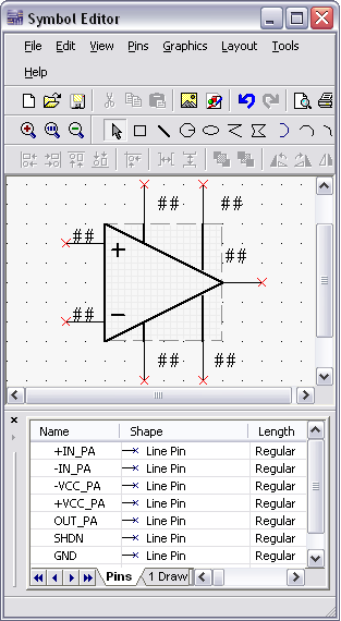
Figure 5. Symbol Editor.
- Select File»Exit to close the Symbol Editor, if asked to save changes choose Yes. The pre-amplifier symbol will now be displayed in the preview box (Figure 6).
If you plan to share this component with colleagues around the world, it is a good idea to create both ANSI and DIN symbols for the device. In this case, simply click on the Copy to button, then select Section A (DIN).
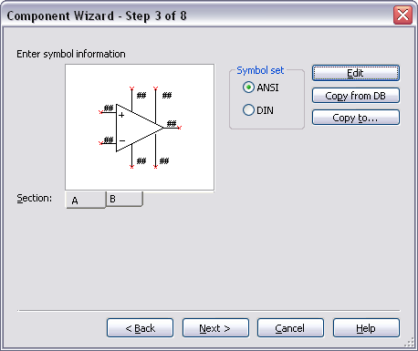
Figure 6. Pre-amplifier symbol.
Assign a symbol for the programmable gain amplifier section:
- Select B in the Section field.
- Click on Edit to open the Symbol Editor.
- Open the file pg_amp.sym.
- Select File»Exit to close the Symbol Editor, if asked to save changes choose Yes. The pre-amplifier symbol will now be displayed in the preview box as shown below:
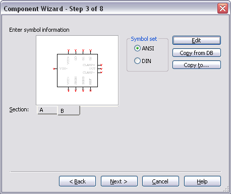
Figure 7. Programmable gain amplifier symbol.
- Click Next to continue.
Step 4: Set Pin Parameters
In this step you can select the pin model type (input, output, and so on) for each pin in the symbol. You can also configure whether to include or exclude that pin from Electrical Rules Check (ERC). If needed, you can add hidden pins to components in this step. Hidden pins are pins that do not appear on the symbol but may be used by the model and/or the footprint.
- Configure the Section and Type columns as shown in the following figure:
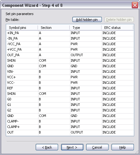
Figure 8. Pin parameters.
- Click Next to continue.
Step 5: Set Mapping Information between Symbol and Layout Footprint
Map visible symbol pins and hidden pins to the PCB footprint. Ensure that the mapping is accurate by comparing it to the datasheet information.
Note: Simulation-only parts do not require this step.
- Click the corresponding Footprint pins cell for each row and assign a pin number. The configured window will look like Figure 9. Note that pins 1 and 17 shared pins.
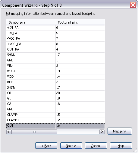
Figure 9. Mapping information between symbol and layout.
- Click Next to continue.
Step 6: Select the Simulation Model
When creating a component for simulation, you must provide the simulation models for each section. You can obtain or create new models in four ways:
- Download a SPICE model from a manufacturer website or other source.
- Manually create a subcircuit or primitive model.
- Use a Multisim Model Maker.
- Or edit an existing model.
Multisim provides Model Makers that create SPICE models for several categories of components based on their databook values. Model Makers exist for operational amplifiers, bipolar junction transistors, diodes, waveguides, and many others. For more information on the various Model Makers, consult the Multisim help file.
For the THS7001, you will use manufacture-provided SPICE compatible models. There are separate models for the pre-amplifier and the programmable gain amplifier sections. They can be found in the Downloads section.
Note: If you are creating a layout-only component, you are not required to complete steps 6 and 7.
- Select the A tab in the Section field.
- Click on Load from file.
- Open the file ths7001_preamp.cir. The SPICE model for the pre-amplifier will load and be displayed in the tab for section A as shown below:
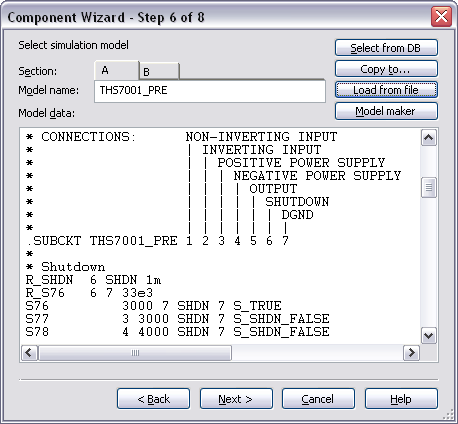
Figure 10. SPICE model for the pre-amplifier section.
- Select the B tab in the Section field.
- Click on Load from file.
- Open the file ths7001_pga.cir. The SPICE model for the programmable gain amplifier will be loaded.
- Click Next to continue.
Step 7: Map Symbol Pins to the Model Nodes
You must map the symbol pins to the SPICE model nodes in order for Multisim to correctly simulate the component. For all subcircuit or macro models, the model nodes are typically documented in the header text of the SPICE model. There is also a line that declares that the model is a subcircuit model and lists the model name followed by the model nodes that will connect to external circuitry.
For the THS7001, the model nodes of the pre-amplifier and the programmable gain amplifier are listed in the files ths7001_pga.cir and ths7001_preamp.cir. You can open these files in a text editor.
Let us examine the header and subcircuit (SUBCKT) lines for the pre-amplifier:
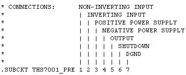
The .SUBCKT line declares that the model is a subcircuit model, lists the name of the model, and displays the external nodes. The comment lines (SHUTDOWN, OUTPUT, and so on) describe the order and operation of the model nodes.
- Complete the pin mapping table for the pre-amplifier (section A) as shown in Figure 11. You must select the Model nodes based on the order in which they appear in the SUBCKT line.
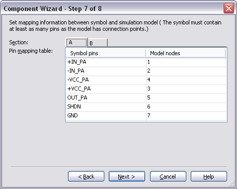
Figure 11. Section A pin mapping table.
- Select Section B and complete the pin mapping table according to the following figure:
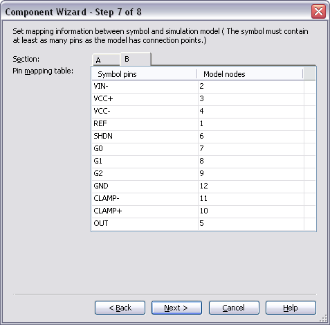
Figure 12. Section B pin mapping table.
- Click Next to continue.
9. Step 8: Save Component into the Database
Once all the previous steps are complete, save the component to the User or Corporate Database.
- Expand the User Database.
- Select the Analog group.
- Click Add Family and type Amplifiers as the new family name.
- Click OK.
- Highlight the new Amplifiers family as shown below:
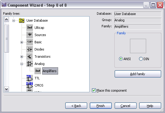
Figure 13. Saving the component to the database.
- Click Finish and place your custom component (Sections A and B) on the Multisim workspace area.
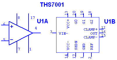
Figure 14. THS7001 Sections A and B.
10. Testing the New Component in Multisim
After creating and saving the custom component, it is available for use in Multisim. To test this component, use the test_circuit.ms11 file located in the Downloads section. Replace U2A with section A of your new component and replace U2B with section B. To replace a component, double-click on the component and then select Replace. Then navigate to the database and location that you saved your component and select it.
Figure 15 illustrates the expected response of the test circuit.
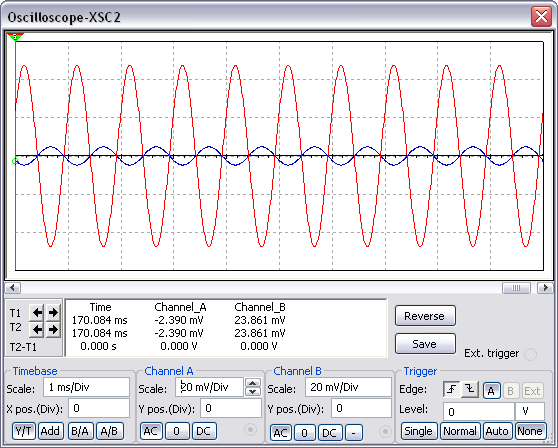
Figure 15. Time domain response of the PGA with Gain set to 111.
